Business

Business Area

홈 · 사업분야 · Applications

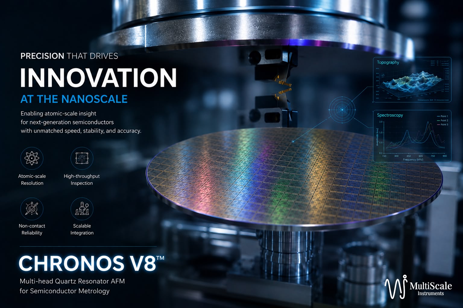
Semiconductor Metrology & Inspection (MI)

 Atomic-level ultra-high resolution analysis

We perform precision analysis of surface characteristics for memory and system semiconductors at the atomic level, delivering high-fidelity 3D data.


 Next-generation inline measurement solutions

We provide non-destructive 3D inline metrology solutions applicable to both Front-End (FE) and Back-End (BE) processes,based on Critical Dimension (CD) measurement and nanoscale surface analysis.

1) Semiconductor & Electronics

 We provide high-precision surface and dimensional metrology for semiconductor wafers, devices, and micro- and nanoscale structures.

Our solutions support process R&D, device inspection, defect analysis, and advanced semiconductor manufacturing development.

2) Research Institutes & Universities

We support fundamental and applied research across nanotechnology, materials science, physics, and engineering.

High-resolution characterization enables detailed investigation of nanoscale structures, surface phenomena, and emerging materials.

3) Advanced Materials & Precision Engineering

We enable precise evaluation of surface morphology, nanostructures, and ultra-precision surfaces.

Our measurement solutions support the development and optimization of advanced materials, functional surfaces, precision components, and next-generation manufacturing technologies.

4) Biomedical & Pharmaceutical

We support nanoscale characterization for biomedical research, medical diagnostics, pharmaceutical development, and nano-bio applications.

Our technology enables detailed investigation of biological materials, surface interactions, and micro- and nanoscale structures relevant to life science research.

Multiscale Instruments, a leader in nano-measurement

This is a staging environment